Overview of OpenPET Framework
Introduction
This document describes the OpenPET electronics system in order to help enable other individuals to contribute to the development of this system. The purpose of the OpenPET electronics is to provide a system that can be used by a large variety of users, primarily people who are developing prototype nuclear medical imaging systems. These electronics must be extremely flexible, as the type of detector, camera geometry, definition of event words, and algorithm for creating the event word given the detector outputs will vary from camera to camera. This implies that users must be able to modify the electronics easily, which further implies that they have easy access to documentation, including the schematics and documents needed to fabricate the circuit boards (Gerber files, bill of materials, etc.) and source code (for both firmware and software). They also need support in the form of instructions, user manuals, and a knowledge base, and they want fabricated circuit boards to be readily available.
The OpenPET system includes “open source” hardware, firmware, and software that will be expanded by LBNL with the help of an active community of developers.
System Overview
The OpenPET system architecture is shown in Fig. 1. There are four types of custom electronics boards in the system: the Detector Board (DB), the Support Board (SB), the Coincidence Interface Board (CI), and the Multiplexer Board (MB). The Support Board plays two roles in the system, depending on the firmware.
The general data flow is that analog signals from detector modules provide the inputs to the Detector Board. This board processes the analog signals to create a singles event word, which is a digital representation of this single gamma ray interaction. The singles event words are passed to the Support Board loaded with detection firmware, whose main function here is to multiplex the singles event words from multiple Detector Boards. The singles event words are then passed through the Coincidence Interface Board to the Multiplexer Board, which can provide a further layer of multiplexing for singles event words, if necessary. Next the multiplexed singles event words are passed to another Support Board loaded with coincidence firmware, which searches through the singles event words for pairs that are in time coincidence and then forms coincidence event words. These coincidence event words are then passed to the Host PC. Optionally, the Support Board with coincidence firmware can act as a multiplexer and pass unaltered singles event words to the Host PC.
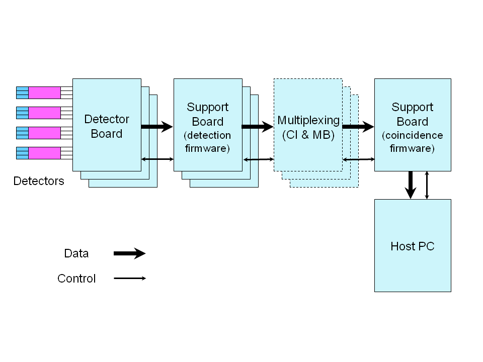
Fig. 1 Schematic of the OpenPET system architecture.
The OpenPET components are housed in an assembly whose form factor is the same as a 12-slot VME crate that accommodates 6U boards. A Support Board essentially replaces the backplane of the VME crate and all the other boards plug into it. The plug-in boards have the same form factor as a VME 6U board, except that the position of the connectors is offset (compared to true VME boards) to prevent OpenPET boards from being plugged into standard VME systems and vice versa.
Definitions
Support Crate
A Support Crate (Fig. 2) is conceptually similar to a VME crate (with controller), namely an intelligent support structure that “functional” boards can be plugged into. It consists of a mechanical frame with 12 plug-in slots, a Support Board (that has a considerable amount of programmable processing power and also acts as a backplane), power supplies, cooling fans, and appropriate boards plugged into slots 9-11. Slots 0-8 are vacant. Slot 9 holds a Host PC Interface Board, which is used to communicate with the Host PC; this board is optional. Slot 10 holds a User IO Board, which allows users to interface to external components such as EKG signals and motor controllers; this board is optional. Slot 11 holds a Debugging Board, which has interfaces to logic analyzers, a number of diagnostic LEDs, an external clock input, and a JTAG connector; this board is optional. Some ancillary components (such as DRAM memory and a QuickUSB board) are also necessary for a functioning Support Crate. By programming the Support Board with appropriate (but different) firmware, the Support Crate becomes part of either a Detector Unit or a Coincidence Unit.
Detector Unit
A Detector Unit (DU), as shown in Fig. 2, consists of a Support Crate with between one and eight Detector Boards plugged into slots 0-7. Each Detector Board can process up to 32 analog input signals. A Detector Unit can therefore process up to 256 analog signals, which corresponds to 64 conventional block detector modules with 4 analog outputs per module. In a Small System (Fig. 5), Slot 8 is typically empty (if data is transferred to the host computer through USB or Ethernet via the Host PC Interface Board plugged into Slot 9). In a Standard (Fig. 4) or Large System (Fig. 5), a Coincidence Interface Board must be plugged into Slot 8 of the Detector Unit. There are two versions of the Coincidence Interface Board: Coincidence Interface Board-1 (CI-1) for the Standard System and Coincidence Interface Board-8 (CI-8) for the Large System. At present, the Coincidence Interface Board-8 has not been designed or specified. These boards transfer event data and bidirectional control data between the Detector Unit and a Coincidence Unit.
In a Detector Unit, the Support Board that acts as a backplane for the Support Crate is loaded with detection firmware. In this case, the Support Board with related firmware and software is called a Detector Unit Controller (DUC).
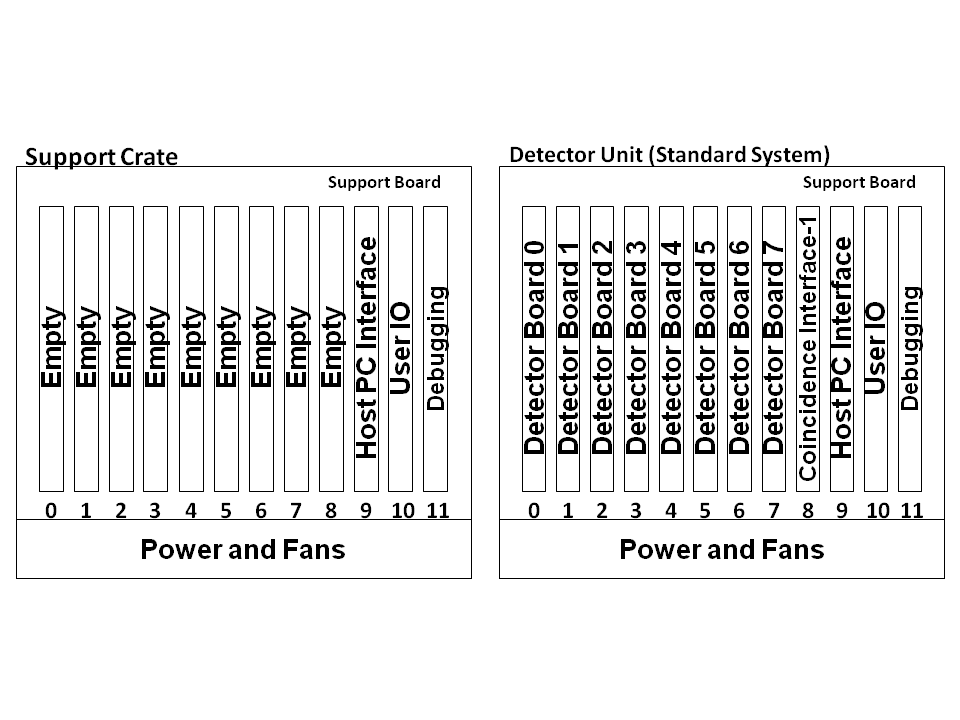
Fig. 2 Support Crate (left) and Detector Unit (right). A Detector Unit is a Support Crate with up to 8 Detector Boards (in Slots 0-7). For a Small System, Slot 8 is usually empty. For Standard and Large Systems, a Coincidence Interface Board must be plugged into Slot 8.
In a Small System, the Support Board in the Detector Unit is programmed to multiplex outputs from the Detector Boards, process coincident events, and pass the coincident events to the host computer. It can also be programmed to multiplex singles events and pass them to the host computer. In a Standard or Large System, the Support Board in the Detector Unit is programmed to multiplex singles events from the Detector Boards and forward them to a Coincidence Unit, as shown in Fig. 4 and Fig. 5. In this specialized case, the Support Board with related firmware and software is called a Coincidence/Detector Unit Controller (CDUC).
Coincidence Unit
The Coincidence Unit (CU) for a Standard System consists of a Support Crate with between one and eight Multiplexer Boards plugged into slots 0-7. The Support Board is loaded with firmware to perform the coincidence processing. Each Multiplexer Board communicates with one Detector Unit via the Coincidence Interface Board using a cable. Similar to the Coincidence Interface Board, there are two versions of the Multiplexer Board: Multiplexer Board-1 (MB-1) for the Standard System and Multiplexer Board-8 (MB-8) for the Large System. At present, the Multiplexer Board-8 has not been designed or specified. The Coincidence Unit’s Support Board is programmed to do the coincidence processing and pass the coincident events to the host computer, although it can also function as a multiplexer and forward singles events. Data is transferred to the Host PC either through USB or Ethernet via the Host PC Interface Board plugged into Slot 9.
In a Coincidence Unit, the Support Board that acts as a backplane for the Support Crate is loaded with coincidence firmware. In this case, the Support Board with related firmware and software is called a Coincidence Unit Controller (CUC).
In the Coincidence Unit for the Standard System, each MB-1 connects with only one Detector Unit via a single cable, allowing up to 64 Detector Boards (or 512 block detector modules) in the system. In the Coincidence Unit for a Large System, the MB-8s plugged into slots 0-7 connect via cables (one cable per Detector Unit) with up to 8 Detector Units, allowing up to 512 Detector Boards (or 4096 block detector modules) in the system. The MB-8s are programmed to serve as multiplexers for events coming from up to 8 Detector Units. Due to the nature of multiplexing, this allows a larger number of channels to be serviced without increasing the maximum total event rate (singles or coincidence).
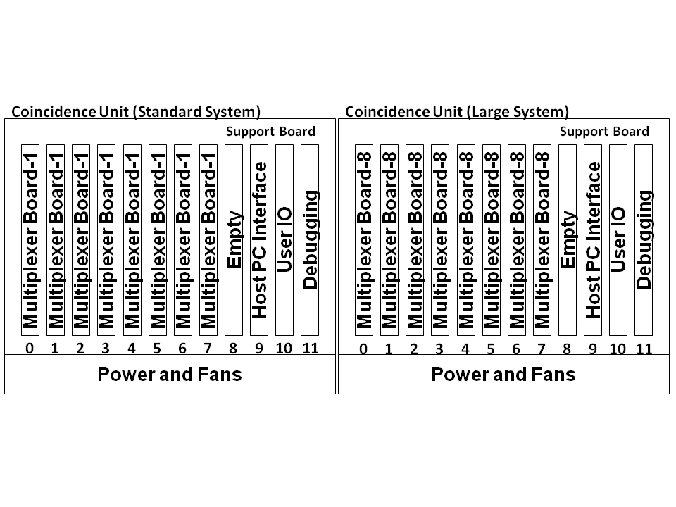
Fig. 3 Coincidence Unit for a Standard System (left) and Large System (right). For both Standard and Large Systems, a Coincidence Unit is a Support Crate with up to 8 Multiplexer Boards (in slots 0-7). In a Large System, the Multiplexer Boards function as multiplexers.
OpenPET can be configured either as a Small System (Fig. 5), Standard System (Fig. 4), or Large System (Fig. 5), with the difference largely due to the number of analog signals that can be read out. To determine which system configuration you need, see the User’s Guide System Configuration section.
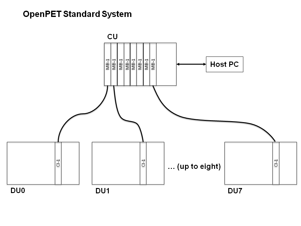
Fig. 4 Configuration of an OpenPET Standard System. Slots 0-7 in the Coincidence Unit contains a Multiplexer Board-1 that services a single DU. Slot 8 in the Detector Unit contains a Coincidence Interface Board-1 that transfers event data and bidirectional control between the DU and CU.
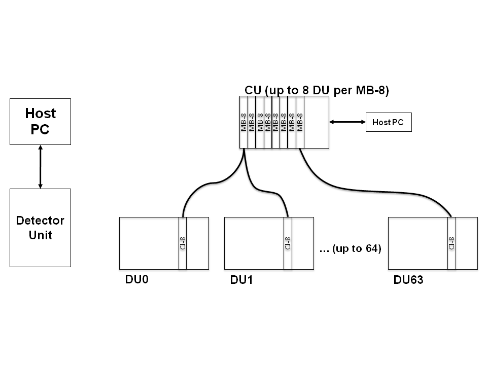
Fig. 5 Configuration of an OpenPET Small System (left) and a Large System (right). In a Small System, the Support Board in the Detector Unit performs the coincidence processing. In a Large System, each of slots 0-7 in the Coincidence Unit contains a Multiplexer Board-8 that functions as a multiplexer and services between 1 and 8 Detector Units. Slot 8 in the Detector Unit contains a Coincidence Interface Board-8 that transfers event data and bidirectional control between the DU and CU.
System Hardware, Firmware, and Software Structures
System Hardware Structure
The basic hardware structure for a standard OpenPET system is shown in Fig. 6.
The host computer is equipped with an USB/Ethernet/Fiber-Optic connection and high-speed hard disk. It sends commands through USB/Ethernet/Fiber-Optic to the Coincidence Unit via the Host PC Interface board. It reads data from the Coincidence Unit through USB/Ethernet/Fiber-Optic and saves them to the hard disk in real time. Currently only a USB communication interface with the host computer has been implemented.
The command bus is shown in red in Fig. 6. Four LVTTL single ended lines are used to pass bi-directional command data between the boards. This command bus uses a custom serial digital bus protocol, consisting of a Clock line (CLK), Data In line (DI), Data Out line (DO), and Chip Selection line (CS). In the current protocol, the Chip Selection line is not utilized.
The data bus is shown in blue in Fig. 6. Sixteen LVDS differential pairs are used to transfer list mode data upstream from the Detector Boards to the host computer.
In the general data flow, analog signals from detector modules are inputted into a Detector Board, which processes these analog signals to create a digital singles event word. The singles event words are passed to a Support Board loaded with detection firmware (SB-DUC), which multiplexes the singles event words from up to eight Detector Boards. The singles event words are then passed through a Coincidence Interface Board to a Multiplexer Board, which can provide a further layer of multiplexing for singles event words, if necessary. Next the multiplexed singles event words are passed to another Support Board loaded with coincidence firmware (SB-CUC), which searches through the singles event words from up to eight Multiplexer Boards for pairs that are in time coincidence and then forms coincidence event words. These coincidence event words are then passed to the host computer. Optionally, the Support Board with coincidence firmware can act as a multiplexer and pass unaltered singles event words to the host computer.
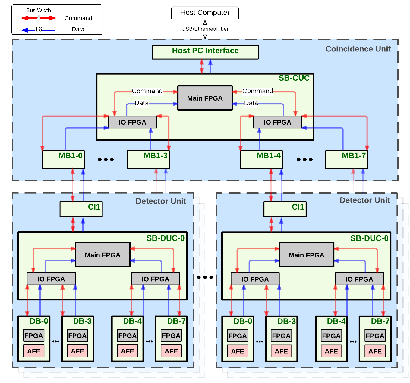
Fig. 6 Standard system hardware structure.
Each Detector Board has an Analog Front End (AFE) and a single Field-Programmable Gate Array (FPGA), as shown in Fig. 6.
Several versions of the Detector Board will be designed, which will differ in how the analog inputs are processed by the front-end circuitries and in the number of analog input channels per Detector Board. The details of each design is described separately in Detector Board. In general, the Analog Front End includes circuitries for analog signal conditioning, analog-to-digital conversion, constant fraction or raising edge discrimination, and timing-to-digital conversion. The Detector Board FPGA performs the necessary computation for event processing, debugging, testing, and calibration tasks. Four single LVTTL lines are used to program the Detector Board FPGA using the custom serial digital bus protocol described above. These signals are provided by the Support Board.
Each Support Board uses three FPGA: a master FPGA (Main FPGA) and two slave FPGAs (IO FPGA). The event multiplexing and forwarding is shared among the three FPGAs due to limited pin count.
The Support Board Main FPGA performs the logical functions of both the master FPGA and the support microprocessor. As the master FPGA, it primarily passes events from the slave IO FPGAs to the Coincidence Interface Board. As a support microprocessor, Nios II is used to program logical blocks in the FPGA to run executable files programmed in C. It is responsible for loading all firmware into the slave FPGAs and Detector Board FPGA, as well as the contents of other registers that are on the DB and SB. For instance, the support microprocessor interprets high-level commands sent from the host computer and executes these commands. This execution may involve controlling the Detector Board, such as by loading firmware into the DB FPGA on the DB; or it may involve higher-level functions, such as performing a calibration by instructing the DB to produce calibration data, analyzing the forthcoming calibration events, computing calibration parameters, and loading these parameters into the detector memory on the DB. It also monitors the event stream and can insert diagnostic information (such as event rates) into the event stream.
The slave IO FPGA passes events to the Main FPGA in different ways depending on the mode of the system. In Scope mode, it queues all the events with no loss of data. For singles events, the IO FPGA acts primarily as a arbitrator, taking up to 16 individual singles events in a single time frame and passing up to four of them to the master FPGA. Clearly some loss results, and the multiplexing algorithm is designed to ensure that this loss is unbiased. Each IO FPGA also serves as a fan-in / fan-out for communication between the support microprocessor and the individual Detector Boards, and the two IO FPGAs can communicate with each other. The digital signals between each IO FPGA and the Main FPGA are identical to the bus IO signals between the IO FPGA and a single Detector Board (see Timing Signals).
System Firmware and Software Structure
(Software: expand on User Guide section 1.4 and Framework section 1.3.2?? Also see details in Framework section 4.
Firmware: expand on User Guide section 1.4 and Framework section 1.3.2?? Also see details in Framework section 5.)
The OpenPET firmware and software structures are based on a computer network tree topology. The configuration strategy needs to fulfill the following two basic requirements:
- Compatibility with different types of detector modules (e.g., single analog channel addressing, single crystal addressing for a conventional block detector, etc.);
- Compatibility with different sized systems (e.g., Small, Standard and Large Systems).
In addition, the configuration strategy needs to be implementable, flexible and reliable.
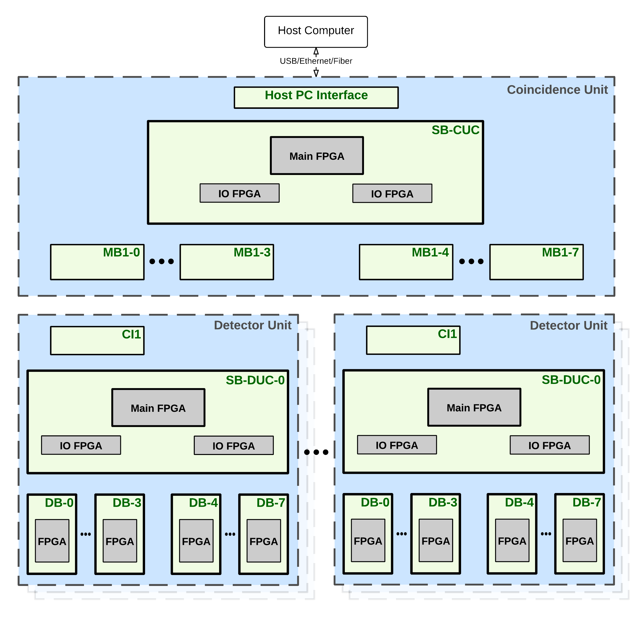
Fig. 7 Standard system firmware and software structure.
The firmware and software structure is shown in Fig. 7, corresponding to the hardware structure shown in Fig. 6. As described in the previous section, All FPGAs (two on supportboard and one on detectorboard) implement software (using NIOS II soft core) and firmware using HDL. The Support Board loaded with coincidence firmware and software is called the Coincidence Unit Controller (CUC). The Support Board loaded with detection firmware and software is called the Detector Unit Controller (DUC).
The computer network tree topology structure is such that the Host PC is the top level and the Detector Boards are the bottom level. The command flow follows a specific path from the source to its destination by writing a specific source and destination address in the system command line. The current OpenPET system uses a 80-bit command word (can be extended) that includes the 16-bit command ID, the 16-bit source and the 16-bit destination addresses, and the 32-bit payload. For a detailed discussion, see System Commands and Responses.
The source address is a 16-bit number that defines where the command originates. Typically, commands that originate at the Host PC have a source address of 0x4000. The destination address is a 16-bit number that identifies where the response should be received and processed. Both the source and destination addresses have the same address format, as shown in Fig. 8.
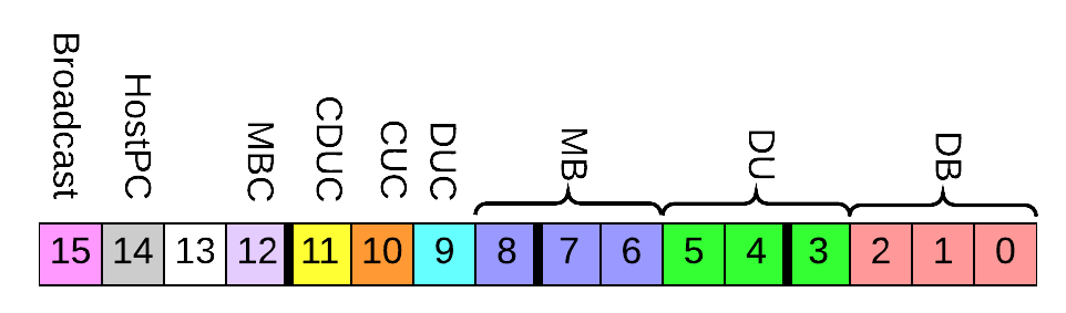
Fig. 8 Source/Destination address (16-bits)
Starting from least significant bit (LSB):
(2:0)   Detector Board Address
(5:3)   Detector Unit Address
(8:6)   Multiplexer Board Address
(9)     Detector Unit Controller source/destination flag
(10)    Coincidence Unit Controller source/destination flag
(11)    Coincidence Detector Unit Controller source/destination flag
(12)    Multiplexer Board Controller source/destination flag
(13)    Not used
(14)    Host PC source/destination flag
(15)    Broadcast flag
As an example, if the Host PC sends a command, the source address Host PC flag bit will be set to 1. The Host PC can talk to any of the components lower on the network by specifying the destination address. If the Host PC needs to send a command to the SB-CUC, the CUC flag in the destination address is set to one. However, if the Host PC wants to communicate with a specific detector board, the full address including the multiplexer board, detector unit and detector board address will be set so that the correct detector board will receive the command. The Host PC is the only node that can initiate commands. The components in the network tree below the Host PC can only reply.
If the Broadcast flag is set in the destination address, the source node will pass the command down to all of its “children” and the child specified in the destination address will be used to create the response.
If the CUC or CDUC flags are set in the destination address, that corresponding unit will execute the command and respond. Since there is no specific address required to send a command to the CUC or CDUC, any address listed is ignored. If the DUC flag is set, only the multiplexer board address is taken into account since a specific DUC corresponds to a specific multiplexer board.
Fig. 9 illustrates the structure of the firmware that exists on all FPGAs in the system.
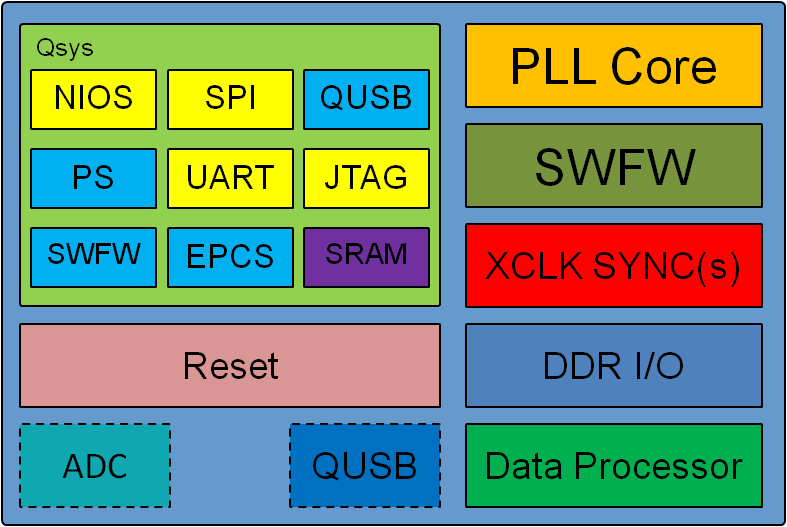
Fig. 9 Block diagram of firmware
The blocks with dotted lines denote aspects located in only specific components of the system. The ADC module exists only on the Detector Board FPGAs, and the QUSB module is only for the top node, for example CDUC. The Qsys subsystem component is provided by Altera and it currently uses the Avalon interface to communicate between its component. A customized SRAM module acts as an Avalon Slave is developed for OpenPET system in house due to the lack of compatible modules provided by Altera. The four blue blocks represent parallel I/O modules.The Reset block is a custom HDL logic used on all FPGAs. The data processor component contains HDL logic for the system mode such as singles mode or scope mode. DDR I/O block is a custom HDL logic which instantiates Altera’s DDR megafunction to allow us to use double data rate transmission on the backplane of the SupportBoard. XCLK Sync(s) are custom HDL cores used to transfer clocks from one domain to the other. SWFW is a custom core used to allow the software running on Nios II to communicate with the firmware fabric. Finally, PLL core is an Altera megafunction with the same configuration settings on all FPGAs.
As far as compatibility with different sized systems, there are two other size options that deviate from the Standard System size. The first is a Small System which consists of a single detector unit with up to eight detector boards. The Support Board on the detector unit is loaded with both coincidence and detection firmware and software and thereby called a Coincidence/Detector Unit Controller (CDUC). The other system size is the Large System which is currently being developed.